
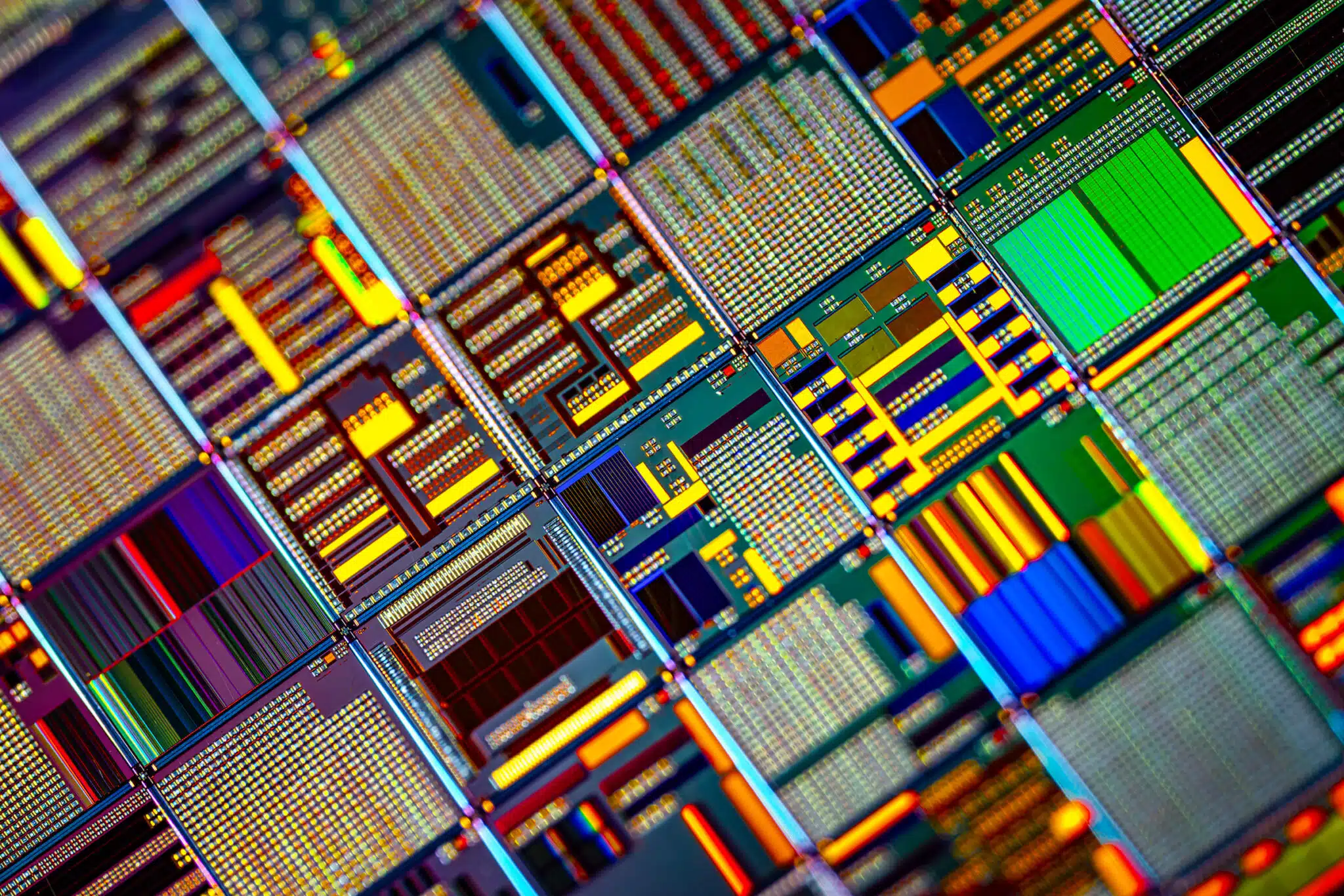
Advanced packaging moved the hardest part of semiconductor manufacturing out of the fab and into assembly. Stacking dies, shrinking interconnects and putting more function into a single package all raise the same question at every step: is what we just built within tolerance, and how would we know? Inspection in packaging is not a final gate. It is a series of measurements taken while the package is still being assembled, when a defect can still be caught cheaply.
What Advanced Packaging Changed About Inspection
Board-level inspection deals in millimetres and hundreds of microns. Packaging deals in tens of microns and below, and the features are often reflective, transparent, or both.
A micro-bump 50 microns across does not tolerate the measurement error that a solder joint on a printed circuit board absorbs without consequence. Nor do the defect modes translate. A package fails through bump height variation, die tilt, cracking, chipping, warpage and foreign material, and most of those are invisible to a system that compares an image against a reference picture. They are geometry problems, and geometry has to be measured.
That is why packaging inspection is built around true 3D measurement with sub-micron height resolution rather than image comparison. The output has to be a number precise enough to act on.
The Measurement Points in a Packaging Line
Wafer level. Before singulation, bumps and pillars are measured across the whole wafer. Systems working at this stage handle 300 millimetre wafers at around 14 wafers an hour, resolving height to between 0.1 and 0.37 microns with height accuracy under 1 micron, and operate in a Class 1000 ISO 6 cleanroom. Our ZenStar overview covers wafer-level packaging inspection in more detail.
Solder and flux, before assembly. Micro solder deposits, bumps and solder balls are measured for height, diameter and volume. The Meister S resolves 5 microns in XY and 0.1 microns in Z across a 20 by 15 millimetre field, at 300 mm²/sec, handling bumps from 20 to 150 microns tall and down to 70 microns in diameter, with warp compensation of plus or minus 5 millimetres.
Transparent flux and warpage. Transparent material is the case that defeats most optical systems, because there is little contrast to work with. The Meister S+ works at 3.5 microns in XY and 0.1 microns in Z, reaching 650 mm²/sec, measures bumps down to 50 microns in diameter, and adds transparent flux inspection with 3D Z-tracking and 2D pad referencing.
Die attach. After placement, the questions become presence, position, tilt, cracking and chipping. The Meister D measures components down to 100 microns at 1 micron Z resolution and 300 mm²/sec, and handles reflective and transparent die surfaces alike.
Mirror-surface dies. A polished die reflects almost all incident light, which makes it one of the harder objects in electronics to measure optically. The Meister D+ addresses this specifically, working at 25 megapixels and 3.5 microns in XY with full 3D height and tilt measurement at 655 mm²/sec.
Matching the System to the Stage
Three questions narrow the choice.
What are you measuring, and how small is it? Bump diameter is usually the binding constraint. A 70 micron minimum and a 50 micron minimum are different machines, not different settings.
Is the surface cooperative? Transparent flux and mirror-finish dies both need systems built for them. Choosing on throughput alone and discovering the surface problem afterwards is an expensive way to learn this.
Where does the measurement happen? Wafer-level inspection is a cleanroom activity with its own handling requirements. Package-level inspection sits closer to a conventional assembly line. The two are not interchangeable.
Throughput matters, but it is the last question rather than the first. A system that measures the wrong feature quickly is not useful.
Putting Inspection Into a Packaging Line
Two practical constraints decide where inspection can physically sit, and both are easier to design for than to retrofit.
The first is environment. Wafer-level inspection belongs in the cleanroom and the equipment has to be rated for it, which is why ZenStar is specified to Class 1000 ISO 6. Package-level inspection after die attach sits in a more conventional assembly environment, with handling closer to a board line.
The second is what happens to the data. Measuring bump height to a tenth of a micron is only worth the capital if the numbers reach the people and systems that can act on them. In practice that means deciding early whether inspection results feed a process-control layer or stop at a pass and fail decision on the machine, because the integration work is the part that gets deferred and then never done.
Qualification is worth planning for as well. Koh Young’s packaging systems are qualified for mass production by major semiconductor foundries, which shortens the internal approval path but does not remove it. Build the evaluation window into the schedule rather than assuming inspection can be added at the end.
From Measurement to Yield
The reason to measure rather than compare is what the numbers let you do next. Bump height distributions drift before they fail. Die tilt trends in one direction before it produces an open. Warpage is a population characteristic rather than a single-unit defect.
Once inspection produces real geometry for every unit, those trends are visible while they are still trends. That is the difference between sorting good packages from bad and understanding why the bad ones happened, which is the only version of inspection that improves yield rather than merely reporting it. Our semiconductor metrology page covers the measurement side in more depth.
Frequently Asked Questions
Is packaging inspection different from semiconductor inspection?
Packaging inspection is a subset. It covers the assembly steps after the wafer is complete: bumping, die attach, solder and flux, and final package verification. Our semiconductor inspection guide covers the wider discipline.
Can SMT inspection equipment be used for advanced packaging?
No. The measurement ranges are an order of magnitude apart. Board-level systems resolve in tens of microns; packaging systems resolve height to a fraction of a micron.
What accuracy is actually required?
It depends on the feature, but sub-micron height accuracy is the working expectation for bumps and dies. Koh Young’s packaging systems hold height accuracy under 1 micron.
Does inspection slow the line down?
Inline measurement is designed to run at process speed, from 300 mm²/sec on the Meister S and D up to 650 and 655 mm²/sec on the S+ and D+.
How is warpage handled?
Warpage is measured rather than corrected. The Meister S compensates across plus or minus 5 millimetres, which keeps bump measurements valid on substrates that are not flat. Warpage is best treated as a population trend, since it usually appears across a batch before it appears as a failure.
What about transparent flux?
Transparent material gives an optical system almost no contrast to work with. The Meister S+ is built for it, adding transparent flux inspection with 3D Z-tracking and 2D pad referencing rather than relying on surface features that are not there.
Next Steps
If you are scoping inspection for a packaging process, the useful starting point is the smallest feature you need to measure and the surface it sits on. Those two answers narrow the options quickly. Get in touch and we will help you work through it.
Related reading:
Semiconductor inspection · Semiconductor metrology · ZenStar wafer-level inspection


