Seoul, Korea – Koh Young, the industry leader in True 3D™ measurement-based dimensional metrology and inspection solutions, will present its latest advancements for semiconductor and advanced packaging applications in Hall 1 Booth 1086 during SEMICON India 2025 held September 2-4, 2025, at Yashobhoomi (IICC), New Delhi, India.
With nearly 25,000 systems installed at over 3,800 manufacturing sites, Koh Young set the standard in automated optical inspection for the electronics manufacturing industry. Building on that foundation, it expanded into semiconductor manufacturing with higherresolution optics, advanced measurement algorithms, and solutions engineered for metrology and inspection of waferlevel packages (WLP), systeminpackage (SiP), and ultra high-density interconnect applications.
As an exhibitor, Koh Young will highlight how its AIpowered metrology and inspection solutions can help manufacturers meet the exacting demands of advanced packaging and semiconductor processes. From waferlevel to SiP, Koh Young technology delivers accurate, repeatable data to enable smarter process control, higher yields, and supports zerodefect production goals.
Dimensional Metrology for Advanced Packaging
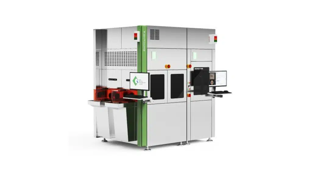
Koh Young’s Meister Series is purposebuilt for advanced packaging, including SiP, WLP, and die stacking metrology. These systems provide ultrahighresolution 2D/3D measurement to manage features and tolerances in nextgeneration designs. Complementing the Meister Series, the ZenStar delivers waferlevel dimensional metrology to detect and quantify critical parameters at the earliest stage, ensuring only knowngood components advance. Together, these platforms help manufacturers maintain process windows, improve yield, and reduce costly rework.
As India accelerates its Make in India semiconductor mission, Koh Young is committed to supporting local and multinational manufacturers in building a competitive, selfreliant ecosystem for advanced electronics. By delivering robust, datadriven metrology and inspection, Koh Young enables domestic production that meets the stringent standards of global supply chains.
“India’s semiconductor industry is entering an unprecedented growth phase,” said Peter Shin, General Manager, Koh Young SouthEast Asia. “Our advanced dimensional metrology and inspection solutions empower manufacturers to deliver worldclass quality, improve productivity, and strengthen India’s position in the global semiconductor market.”
For more information about Koh Young’s semiconductor focused dimensional metrology and inspection systems, visit us at SEMICON India 2025 or online at www.kohyoung.com.
About Koh Young Technology, Inc.
Founded in 2002, Koh Young Technology transformed the inspection market with the industry’s first 3D Solder Paste Inspection (SPI) system using patented dual-projection Moiré technology. Today, Koh Young is the global leader in True3D™ measurement-based SPI and Automated Optical Inspection (AOI) solutions for electronics manufacturing. Building on its core True3D™ technology, Koh Young has expanded its capabilities to address complex inspection challenges, including machined parts, press-fit and through-hole pins, conformal coatings, dispensed materials, and semiconductor packaging. Through continuous innovation and a customer-focused R&D approach, the company has earned the trust of over 3,800 customers worldwide and maintains the dominant global market share with nearly 25,000 systems installed. Headquartered in Korea with regional offices across the globe, Koh Young provides local sales and support to stay close to its markets and growing user base. Electronics manufacturers around the world rely on Koh Young to deliver reliable inspection, actionable process insight, and a pathway to a smarter factory. Learn more about Koh Young’s Semiconductor Metrology Solutions.